- You are here: Home
- Services
- Histology Services
- Scanning Electron Microscopy (SEM)
Services
-
Cell Services
- Cell Line Authentication
- Cell Surface Marker Validation Service
-
Cell Line Testing and Assays
- Toxicology Assay
- Drug-Resistant Cell Models
- Cell Viability Assays
- Cell Proliferation Assays
- Cell Migration Assays
- Soft Agar Colony Formation Assay Service
- SRB Assay
- Cell Apoptosis Assays
- Cell Cycle Assays
- Cell Angiogenesis Assays
- DNA/RNA Extraction
- Custom Cell & Tissue Lysate Service
- Cellular Phosphorylation Assays
- Stability Testing
- Sterility Testing
- Endotoxin Detection and Removal
- Phagocytosis Assays
- Cell-Based Screening and Profiling Services
- 3D-Based Services
- Custom Cell Services
- Cell-based LNP Evaluation
-
Stem Cell Research
- iPSC Generation
- iPSC Characterization
-
iPSC Differentiation
- Neural Stem Cells Differentiation Service from iPSC
- Astrocyte Differentiation Service from iPSC
- Retinal Pigment Epithelium (RPE) Differentiation Service from iPSC
- Cardiomyocyte Differentiation Service from iPSC
- T Cell, NK Cell Differentiation Service from iPSC
- Hepatocyte Differentiation Service from iPSC
- Beta Cell Differentiation Service from iPSC
- Brain Organoid Differentiation Service from iPSC
- Cardiac Organoid Differentiation Service from iPSC
- Kidney Organoid Differentiation Service from iPSC
- GABAnergic Neuron Differentiation Service from iPSC
- Undifferentiated iPSC Detection
- iPSC Gene Editing
- iPSC Expanding Service
- MSC Services
- Stem Cell Assay Development and Screening
- Cell Immortalization
-
ISH/FISH Services
- In Situ Hybridization (ISH) & RNAscope Service
- Fluorescent In Situ Hybridization
- FISH Probe Design, Synthesis and Testing Service
-
FISH Applications
- Multicolor FISH (M-FISH) Analysis
- Chromosome Analysis of ES and iPS Cells
- RNA FISH in Plant Service
- Mouse Model and PDX Analysis (FISH)
- Cell Transplantation Analysis (FISH)
- In Situ Detection of CAR-T Cells & Oncolytic Viruses
- CAR-T/CAR-NK Target Assessment Service (ISH)
- ImmunoFISH Analysis (FISH+IHC)
- Splice Variant Analysis (FISH)
- Telomere Length Analysis (Q-FISH)
- Telomere Length Analysis (qPCR assay)
- FISH Analysis of Microorganisms
- Neoplasms FISH Analysis
- CARD-FISH for Environmental Microorganisms (FISH)
- FISH Quality Control Services
- QuantiGene Plex Assay
- Circulating Tumor Cell (CTC) FISH
- mtRNA Analysis (FISH)
- In Situ Detection of Chemokines/Cytokines
- In Situ Detection of Virus
- Transgene Mapping (FISH)
- Transgene Mapping (Locus Amplification & Sequencing)
- Stable Cell Line Genetic Stability Testing
- Genetic Stability Testing (Locus Amplification & Sequencing + ddPCR)
- Clonality Analysis Service (FISH)
- Karyotyping (G-banded) Service
- Animal Chromosome Analysis (G-banded) Service
- I-FISH Service
- AAV Biodistribution Analysis (RNA ISH)
- Molecular Karyotyping (aCGH)
- Droplet Digital PCR (ddPCR) Service
- Digital ISH Image Quantification and Statistical Analysis
- SCE (Sister Chromatid Exchange) Analysis
- Biosample Services
- Histology Services
- Exosome Research Services
- In Vitro DMPK Services
-
In Vivo DMPK Services
- Pharmacokinetic and Toxicokinetic
- PK/PD Biomarker Analysis
- Bioavailability and Bioequivalence
- Bioanalytical Package
- Metabolite Profiling and Identification
- In Vivo Toxicity Study
- Mass Balance, Excretion and Expired Air Collection
- Administration Routes and Biofluid Sampling
- Quantitative Tissue Distribution
- Target Tissue Exposure
- In Vivo Blood-Brain-Barrier Assay
- Drug Toxicity Services
Scanning Electron Microscopy (SEM)
Scanning Electron Microscopy (SEM) is a cutting-edge imaging technique that utilizes a focused beam of electrons to scan the surface of a sample, producing high-resolution images with exceptional detail. Unlike traditional optical microscopes, SEM can achieve much higher magnifications and provide in-depth information about surface structures, making it an invaluable tool across various fields such as materials science, life sciences, and geology.
With years of experience in the field of electron microscopy, our team of experts is dedicated to providing high-quality SEM services tailored to meet your specific needs. We have successfully collaborated with clients from various industries, including academia, pharmaceuticals, and manufacturing, delivering precise imaging and analysis that drive innovation and research.
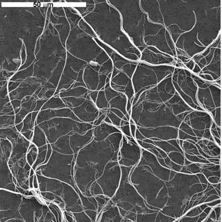 Figure 1. UICC Asbestos Chrysotile 'A' standard.
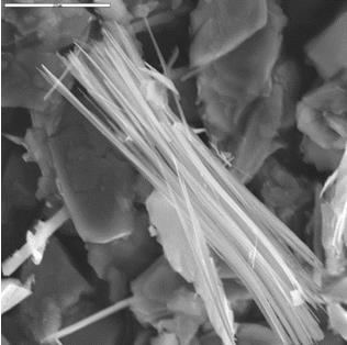 Figure 2. Tremolite asbestos, Death Valley, California
How SEM Works?
SEM operates by directing a focused electron beam onto the surface of a sample, generating a variety of signals, including secondary electrons, backscattered electrons, and characteristic X-rays. These signals are captured by detectors and converted into images that reveal the surface morphology and composition of the sample.
- Sample Preparation: Samples often require conductive treatment to prevent charge accumulation during electron beam exposure.
- Electron Beam Scanning: The electron beam scans the sample surface, collecting signals point by point.
- Image Generation: Signals are processed by a computer to generate high-resolution images.
Applications
- Materials Science: Analyzing microstructures, defects, and compositions of metals, polymers, and composites.
- Biology: Observing the ultrastructure of cells, tissues, and microorganisms for research and diagnostics.
- Geology: Studying the surface features of minerals, rocks, and fossils to understand geological processes.
- Nanotechnology: Characterizing the morphology, size, and distribution of nanomaterials for advanced applications.
- Electronics: Inspecting semiconductor devices and circuit boards for quality control and failure analysis.
Advantages
- High Resolution: SEM provides images with resolutions down to the nanometer scale, allowing for detailed analysis of surface features.
- Depth of Field: The technique offers a greater depth of field compared to optical microscopy, enabling clear imaging of three-dimensional structures.
- Elemental Analysis: SEM can be equipped with Energy Dispersive X-ray Spectroscopy (EDS) for elemental composition analysis, providing valuable insights into material properties.
- Versatility: SEM can be applied to a wide range of materials, including metals, ceramics, polymers, and biological specimens.
Quotation and ordering
Our customer service representatives are available 24hr a day! We thank you for considering Creative Bioarray as your Scanning Electron Microscopy (SEM) Services partner.
Explore Other Options
For research use only. Not for any other purpose.
